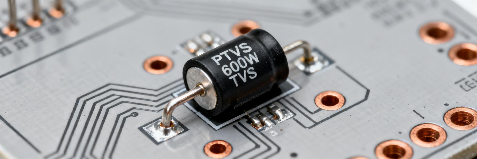
PTVS6V0P1UTP115 TVS Diode: Key Performance & Test Data
The PTVS6V0P1UTP115 delivers high peak-pulse capability (typ. 600 W) and defined single-pulse clamp and surge figures, making measured behavior decisive for protection designs.
Background: What PTVS6V0P1UTP115 Is and Where It's Used

Key specs to note
Point: Designers must extract a set of datasheet-rated values before validation.
Evidence: Nominal standoff (Vr), breakdown range (Vbr), typical clamp voltage (Vclamp), peak-pulse power (600 W class), peak-pulse current (Ipp), package (SOD-128/F), and directionality (uni/bi).
Explanation: These specs determine clamp margin, thermal stress, and suitability for a given rail and define which electrical tests to prioritize when characterizing TVS diode performance.
Typical application contexts
Point: The device class targets transient suppression on low-voltage rails and I/O lines.
Evidence: Common uses include 5–12 V power rails, data-line protection, and industrial/automotive surge zones where single high-energy events occur.
Explanation: Recommended operating windows keep working voltage well below breakdown and apply derating for repeated surges or elevated ambient temperature to preserve lifetime and clamping consistency.
Key Performance Metrics (Data Analysis)
Electrical performance metrics to report
- • Point: A focused metric set yields meaningful comparison to datasheet claims.
- • Evidence: Report standoff (Vr), breakdown (Vbr), Vclamp at defined Ipp points (1 A, 10 A, datasheet Ipp), dynamic resistance (Rd), leakage (IR), junction capacitance (Cj), and time-to-clamp.
- • Explanation: Measuring at 1 A and 10 A plus the rated Ipp reveals nonlinear V-I behavior and is essential for accurate clamping-voltage modeling.
Thermal & reliability indicators
- • Point: Thermal response often limits real-world surge endurance.
- • Evidence: Capture thermal resistance, max junction temperature under pulse, surge cycle endurance, and operating temperature ranges.
- • Explanation: Thermal limits govern repeated-pulse derating; documenting temperature rise per absorbed energy helps predict when cumulative heating will shift Vbr.
Test Methodology & Recommended Setup
Pulse test setup and measurement tips
Point: Accurate Vclamp measurement requires careful setup.
Evidence: Use a pulse generator capable of standard 10/1000 µs or 8/20 µs shapes, include recommended series resistance, place current probe in-line near the device, use >100 MHz scope bandwidth, and measure Vclamp directly across the diode with short leads.
Explanation: Minimizing loop inductance and consistent probe placement reduces overshoot and layout-driven measurement error that otherwise inflates apparent clamp voltage.
Pass/fail criteria and repeatability
Point: Define clear acceptance thresholds and statistical rigor.
Evidence: Set Vclamp acceptance relative to datasheet (for example ±10–15%), leakage ceilings, required pulse counts, cooling intervals, and sample size (≥9–30 parts for batch confidence).
Explanation: Consistent cooling intervals and sample-size rules prevent false fails due to thermal accumulation and reveal manufacturing variability that single-sample tests miss.
Comparative Benchmarks & Example Test Data
| Test | Pulse Type | Ipp (A) | Measured Vclamp (V) | Energy (J) | Temp Rise (°C) |
|---|---|---|---|---|---|
| Short pulse | 8/20 µs | 10 | 9.8 |
|
12 |
| Long pulse | 10/1000 µs | 3 | 7.2 |
|
18 |
| Rated Ipp | Manufacturer Ipp | 50 | 12.4 |
|
45 |
Interpreting deviations and failure modes
Point: Deviations often stem from test setup or part variations. Evidence: Typical signatures include raised leakage, reduced Vbr, or open/short failures after high-energy tests. Explanation: Layout parasitics and probe placement inflate measured Vclamp; consistent increases in leakage or lowered breakdown indicate junction damage.
Design & Application Recommendations
Sizing and derating rules
Maintain reserve between clamped voltage and protected IC absolute max (typ. ≥20–30%), derate energy handling for repeated events, and prefer footprints that improve thermal dissipation to prevent inadvertent overstress during worst-case surges.
Integration tips and verification
Place TVS diode close to protected port with short traces, use low-inductance vias, route return paths carefully, and run in-system ESD, EFT, and surge qualification to capture integration pitfalls before long-term reliability testing.
Summary
- [!] The PTVS6V0P1UTP115 requires measurement of Vclamp at 1 A, 10 A, and datasheet Ipp to validate real TVS diode performance.
- [!] Thermal response and cumulative heating dictate derating; record temp rise per absorbed energy to predict endurance.
- [!] Use a standardized test table and repeatable setup to separate layout-induced artifacts from true device deviations.