PTVS6V5S1UR TVS Diode: Key Specs & Datasheet Guide
Measured peak pulse power of 400 W (350 W for 3.3 V use) and sub-microamp leakage place this unidirectional protector among compact, high-energy transient suppressors for low-voltage rails. This guide outlines practical steps to read the datasheet, assess clamping behavior, and apply the device in PCB designs.
Overview: What PTVS6V5S1UR Is and Where It Fits

Key Electrical Class & Package
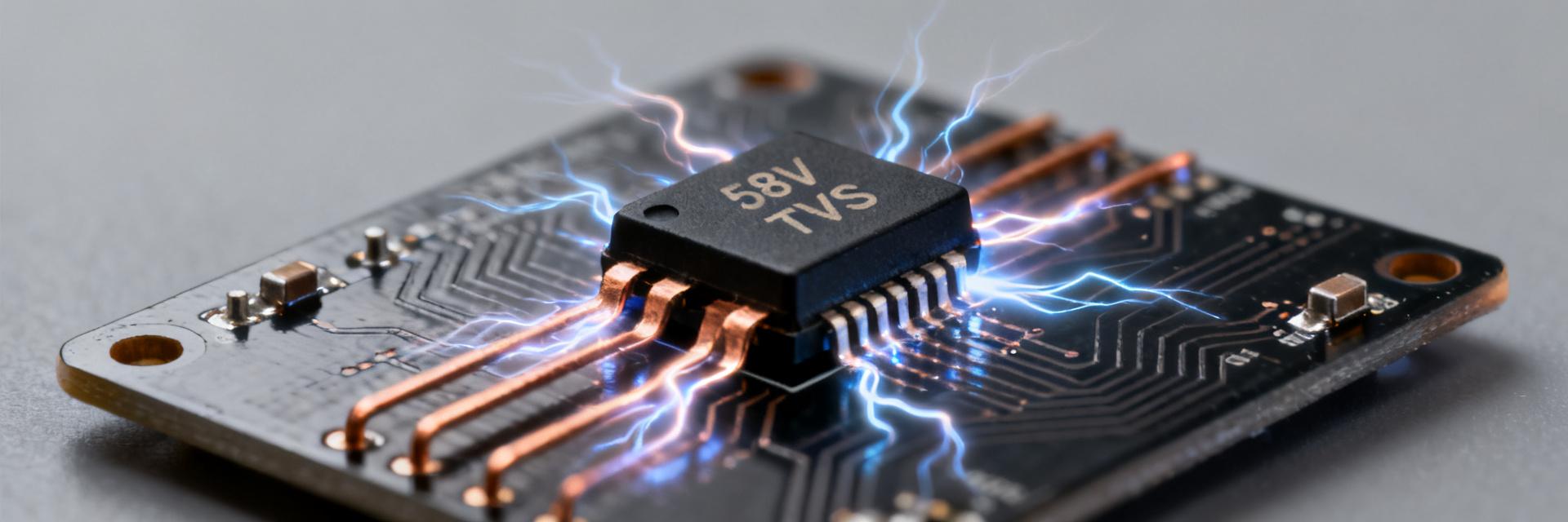
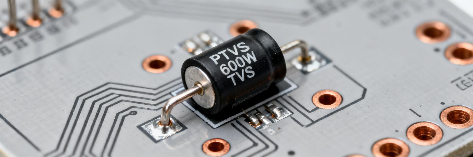
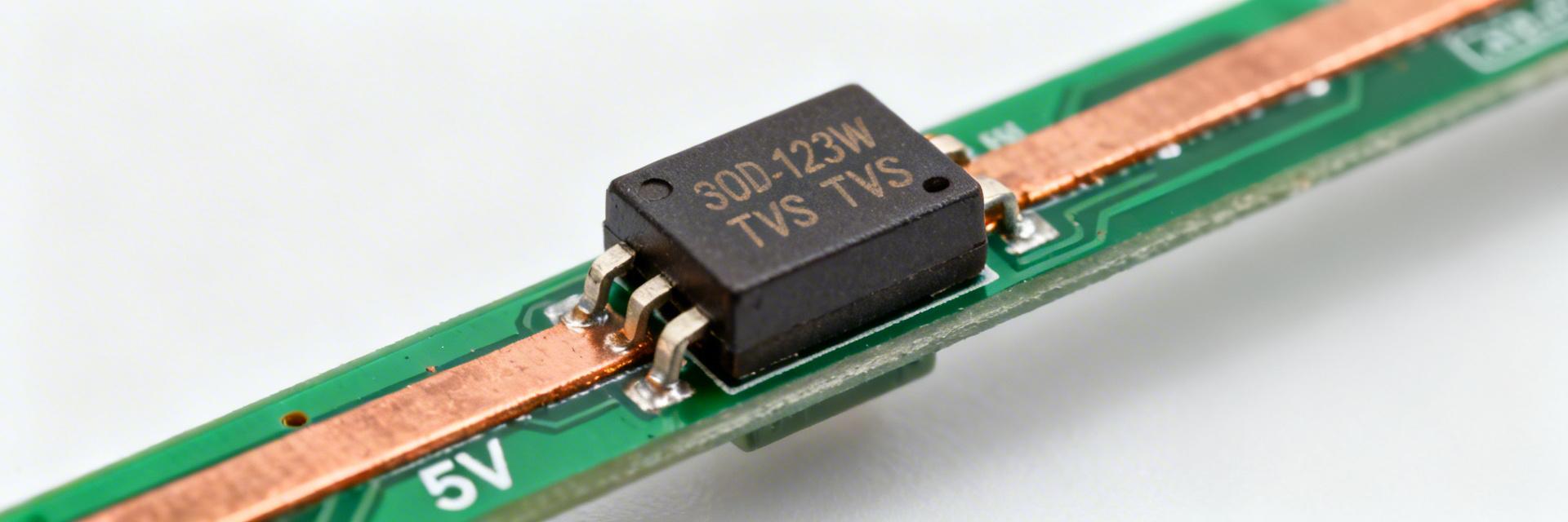
Unidirectional TVS behavior with ~6.5 V VRWM in SOD-123W (CFP3) form factor. This two-terminal SMD features a low profile and small pad footprint. The compact size favors dense PCBs; however, keep traces minimal to reduce inductance and ensure fast clamp action.
Typical Applications
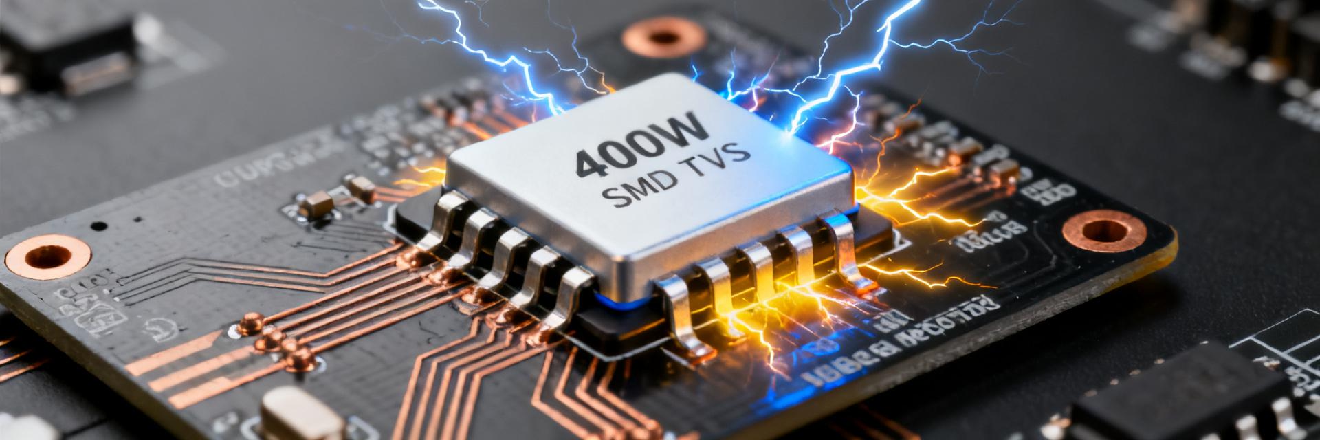
Common uses include 3.3 V power rails, I/O lines, and automotive ancillary circuits. 400 W peak pulse energy supports single high-energy transient events. This capability limits voltage excursions during surges, protecting downstream regulators and sensitive interfaces.
Key Specifications: Quick Spec Sheet Explained
Core Electrical Parameters
| Parameter | Symbol | Typical Value | Visual Scale |
|---|---|---|---|
| Reverse Standoff Voltage | VRWM | 6.5 V |
|
| Breakdown Voltage | VBR | ~7.2 V |
|
| Peak Pulse Power (8/20 µs) | PPP | 400 W |
|
Transient & ESD Resilience
Pulse test conditions (8/20 µs) and ESD ratings determine real-world resilience. PPP rating is measured under standard waveforms; package thermal resistance and max junction temperature define dissipation limits. Confirm surge current and ESD ratings before layout to avoid thermal mismatch.
Datasheet Deep Dive: Reading the PTVS6V5S1UR Datasheet
Electrical Tables & Test Conditions
Locate absolute maximums and characteristics. Tables show VRWM, VBR, IR (leakage), and test waveforms with tp specifications. Footnotes often indicate ambient vs junction testing; translate these to your environment for conservative design margins.
Characteristic Curves
Clamping vs. pulse current curves and power derating are essential. To predict clamp during a surge, pick the expected current on the x-axis and read VC. Apply derating for elevated ambient temperatures or repeated events.
Design & Application Guidelines for Engineers
Layout & Thermal Best Practices
- ✔ Minimize loop inductance by placing the diode adjacent to the connector.
- ✔ Maximize copper pours and use thermal vias to lower thermal resistance.
- ✔ Avoid narrow PCB necks that concentrate heat during a pulse event.
System-Level Strategies
For 3.3 V rails, choose VRWM just above nominal but below component maximums. Consider multi-stage protection (adding series resistance or inductance) to handle repeated or complex surge profiles in harsh environments.
Selecting the Right TVS: Comparison Checklist
Decision Checklist
Verify VRWM vs system voltage, PPP requirements, clamp limits, and footprint. Prioritize low leakage for battery-powered devices and low capacitance for high-speed lines.
When to Switch
Trade-offs include higher power packages or bidirectional parts for AC lines. If repeated high-energy events occur, pair TVS with series PTC or polymeric devices.
Practical Implementation & Troubleshooting
Pre-deployment Validation
Perform bench surge tests (8/20 µs) to verify clamp voltage at expected currents. Document pass/fail thresholds for VC and leakage across operational temperatures.
Common Failure Modes
Orientation errors on unidirectional parts, insufficient copper area, and repeated overstress lead to increased leakage or short circuits. Expand copper pours if failures persist.
Summary
The PTVS6V5S1UR is a compact, high-energy unidirectional TVS diode designed for low-voltage rails with a 400 W peak pulse rating. Success requires careful matching of VRWM to nominal rails, robust thermal layout, and rigorous bench validation.
- Match VRWM: Ensure VC stays safe for downstream components.
- Thermal Design: Use generous copper pours to improve pulse dissipation.
- Validation: Perform surge injections and leakage checks before field use.