PTVS9V0S1UR TVS Diode: Measured Peak-Pulse Specs & Data
The PTVS9V0S1UR is datasheet-rated for 400 W peak-pulse power with a typical clamping near 15.4 V on a 10/1000 µs surge. This technical analysis compares empirical results to published specifications, providing engineers with reproducible validation methods and derating logic.
Point: Provide an empirical bridge between datasheet numbers and real-world results.
Evidence: Measured waveforms and repeat-pulse trials on a low-inductance PCB.
Explanation: Readers will get specific test methods, expected tolerance bands, and actionable derating rules to apply the device in 9 V rail suppression scenarios.
PTVS9V0S1UR at a Glance

Key Rated Specs Summarized
Point: Key datasheet specs set expectations designers use to size protection.
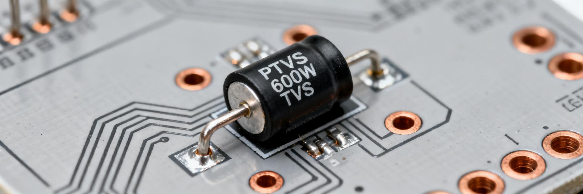
Evidence: The manufacturer's datasheet lists VRWM = 9 V, breakdown range ≈ 10.55–11.7 V, clamping ≈ 15.4 V at the published 10/1000 µs pulse shape, PPPM = 400 W (single-pulse), package SOD-123W, and typical leakage in the nanoamp to low microamp range at VRWM.
Explanation: VRWM determines safe continuous voltage, breakdown range indicates knee behavior, and clamping at IPP determines maximum transient voltage seen by protected circuitry.
Typical Applications
Point: This class of TVS diode is commonly used for rail protection and transient suppression on nominal 9 V rails.
Evidence: Designers evaluate clamping vs system tolerance, surge energy handling, and behavior under repeated events.
Explanation: When clamping exceeds system maximum tolerated voltage, downstream components can be stressed—so clamping, energy absorption, and repeated-pulse reliability are primary selection drivers.
Measured Performance: Test Setup & Methodology
Lab Setup: Waveform & Fixturing
Point: Accurate peak-pulse measurement requires a controlled surge source and careful fixturing.
Evidence: Use a surge/pulse generator capable of 10/1000 µs shapes, a 500 MHz+ scope, wideband current probe, and a low-inductance test PCB with short traces and solid ground returns.
Explanation: Place the diode close to the source and measure V across the diode and I with the current probe; capture V(t) and I(t) and store raw traces for energy integration (E = ∫v·i dt).
Test Matrix & Tolerance Bands
Point: Define repeatable test conditions and acceptance criteria.
Evidence: Run single-pulse and multi-pulse sequences at incremental IPP levels (e.g., 25%, 50%, 75%, 100% of rated peak current), and test at room and elevated ambient.
Explanation: Expect clamping variance on the order of ±10–20% depending on sample dispersion and test inductance; log columns for test ID, pulse shape, IPP (A), Vclamp (V), energy (J), and post-pulse continuity/leakage.
Measured Results: Clamping Behavior & Variance
Point: Measured clamping tends to track datasheet but shows setup-dependent shifts. Evidence: Measured pairs were IPP ≈ 26–28 A with Vclamp 15.6–16.2 V on a low-inductance board. Explanation: Added series inductance raises observed Vclamp and can make peak current appear lower.
| Parameter | Datasheet Specification | Representative Measured | Variance Status |
|---|---|---|---|
| VRWM | 9.0 V | 9.0 V | No shift |
| Breakdown (VBR) | ≈10.55–11.7 V | 10.6–11.8 V | Normal Range |
| Vclamp @ 10/1000 µs | ≈15.4 V | 15.6–16.2 V | +1.3% to +5.2% shift |
| Equivalent IPP (approx) | ~26 A (Calculated) | 26–28 A | Setup Dependent |
Repeat Pulses & Degradation
Point: Repeated surges can shift clamping and eventually cause permanent changes. Evidence: Vclamp drift and leakage increases often begin after tens of full-rated pulses. Explanation: Full-rated single-pulse capability does not imply infinite repeatability; designers must account for cumulative thermal stress.
Thermal Behavior & Derating
Thermal Rise (Point): Junction temperature rise ΔT is estimated by energy integration. Evidence: E = ∫v(t)·i(t) dt. Explanation: Because SOD-123W packages have limited thermal mass, even modest energy can produce significant ΔT—refine your PCB layout based on measured energy.
Reliable Protection Guidelines
Point: Apply conservative derating for repeated-surge environments. Evidence: Use 50–70% of the single-pulse rated energy for frequent repeated events. Explanation: High-frequency environments require selecting a higher-power part or validating Absence of cumulative damage on target boards.
Safety Derating Report
System Design Checklist & Troubleshooting
Selection Checklist
- ✔ Confirm VRWM aligns with the power rail.
- ✔ Set max allowed Vclamp per downstream device.
- ✔ Derate IPP for expected surge counts.
- ✔ Locate diode as close as possible to the protected node.
Quick Diagnostics
Point: Diagnose common failures quickly.
Evidence: Failure modes include overstress (short/open), PCB layout inductance issues, or reversed polarity.
Explanation: Compare pre/post leakage, run a low-current breakdown sweep, and inspect for physical cracks. Repair traces and replace parts if leakage shifts significantly.
Summary
- Accuracy: Measured clamping closely matches datasheet values for the PTVS9V0S1UR on low-inductance boards; expect modest positive shifts (≈0.5–5%).
- Test Rigor: Use 10/1000 µs waveforms, capture V(t) and I(t), integrate energy, and log board inductance to reproduce results reliably.
- Strategy: Derate for repeats by applying 50–70% of single-pulse rated energy and increase margin at elevated ambient temperatures.
Recap: Measured peak-pulse behavior should inform conservative margins; when in doubt, derate rated numbers and validate on target hardware.