PUMB11 Datasheet Deep Dive: Key Specs & Pinout Explained
The PUMB11 datasheet highlights a 50 V Vce rating, a 100 mA collector current limit, and approximately 300 mW steady-state power dissipation. With built-in bias resistors (R1 = 10 kΩ / R2 = 10 kΩ), these specifications directly constrain topology, bias margins, and PCB thermal planning. This deep dive covers device roles, absolute maximums, recommended operating conditions, pinout mapping, and layout checklists to streamline component selection and high-reliability prototyping.
Background: Device Role and Integration

Functional Description
The PUMB11 is a dual PNP transistor featuring integrated base bias resistors. The datasheet specifies a pre-biased architecture with Rbias values of 10 kΩ. This integration simplifies input circuits by providing defined pull paths, reducing external component counts, and improving repeatability for level-shifting tasks while maintaining the flexibility to override bias control via external resistors.
Typical Roles & Systems
Common applications include low-current signal switching, level translation, and complementary stages. The 100 mA collector limit and modest power dissipation favor small loads and interface tasks. For digital interfacing, the Vbe thresholds determine switching logic, guiding whether the PUMB11 acts as a primary switch or a driver for external MOSFET gates.
Key Electrical Specifications
Respecting absolute maximums is critical to preventing immediate or latent semiconductor failure. Below is a visual and tabular breakdown of the primary operational constraints.
Electrical Characteristics Deep Dive
DC Performance: Gain and Leakage
DC parameters drive bias and gain margin. The datasheet provides hFE vs. Ic curves showing that gain varies significantly with collector current and temperature. Designers should account for base-emitter drops (~0.6–0.9 V) when calculating bias networks and include leakage current allowances for high-impedance circuits.
Switching Dynamics and Thermal Management
Dynamic limits determine the switching speed and heat accumulation. This device family targets low-to-moderate-speed signals. For pulse applications, ensure the thermal time constants and average dissipation stay within Pd limits. Use conservative duty cycles or additional copper cooling for frequent high-current switching cycles.
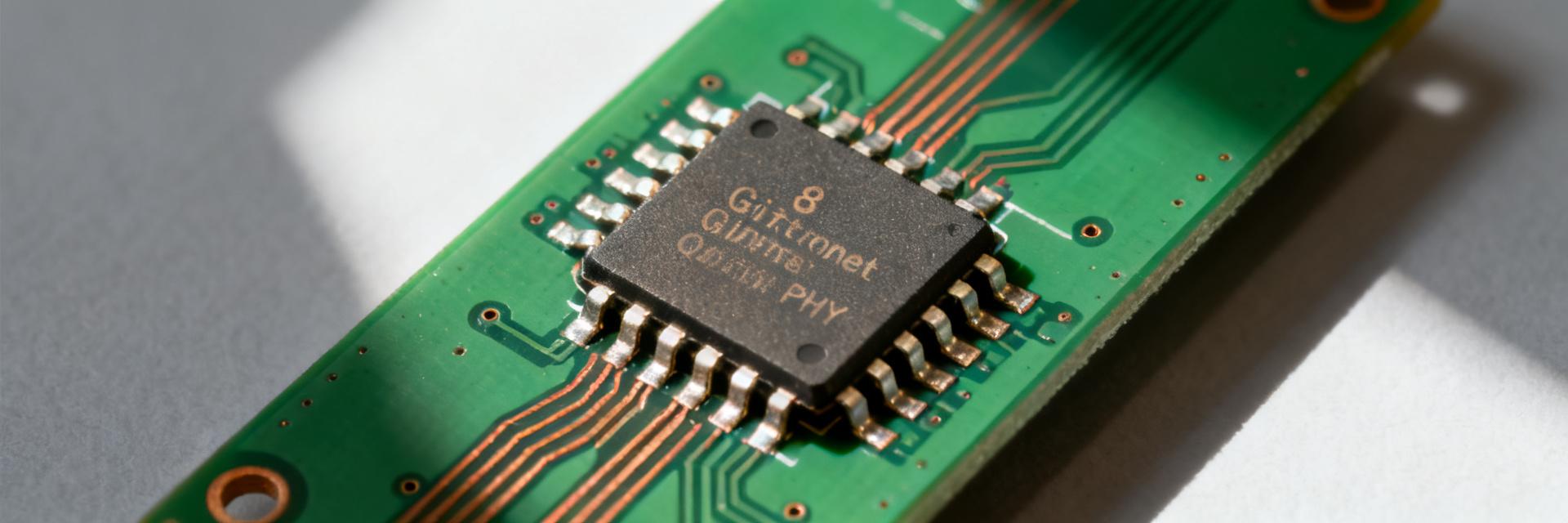
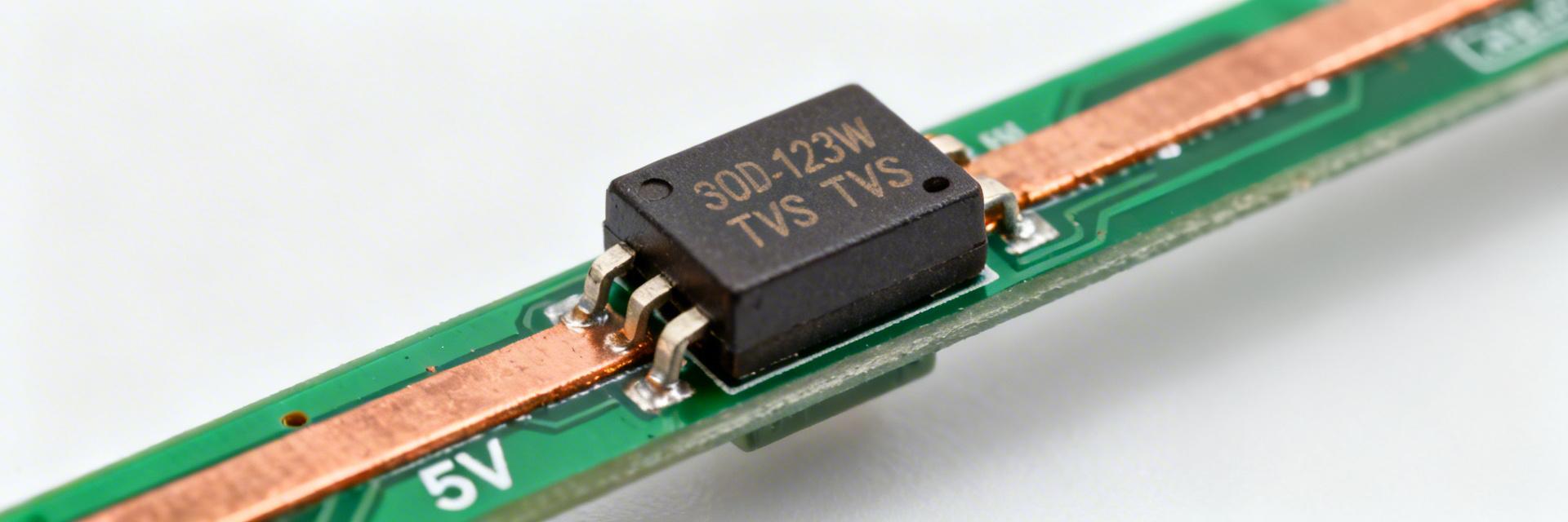
Pinout & Package Insights
Pin Mapping Explained
Correct pin naming is essential to prevent wiring errors. The dual-PNP package assigns specific emitter, base, and collector pins for each transistor.
Pinout Reference:
- Left Transistor: Emitter, Base, Collector
- Right Transistor: Emitter, Base, Collector
- Internal Bias: R1/R2 integrated between bases and reference nodes.
Footprint Tips
Follow the official SMD land-pattern recommendations. To optimize thermal performance, add thermal vias under larger pads where Pd and θJA demand heat spreading. Maintain strict component keepouts to avoid solder bridging and thermal hotspots during reflow.
Application Circuits & Worked Examples
Example: High-Side Switching
To size a base drive for a target Ic = 50 mA, choose a forced beta (e.g., 10–20) so Ib ≈ 2.5–5 mA. Calculate the series base resistor by considering the input voltage, Vbe, and the internal 10 kΩ bias paths. Always confirm that Vce_sat × Ic remains within the 300 mW power limit.
Summary of Design Guidance
- ✓ Verify Vce (50V) and Ic (100mA)
- ✓ Add copper pour for heat spreading
- ✓ Use 10kΩ internal bias logic
Confirm hFE at intended temperature. Use current-limited supplies for initial bring-up to protect against overstress.
Do not use for currents >100 mA or ultra-high-speed switching where internal capacitance limits performance.