


Helping you save cost and time.

Provide reliable packaging for your goods.

Quick and reliable delivery to save time.

Excellent after-sales service.
New Product Launch
More +

Hot Selling Parts


Blog
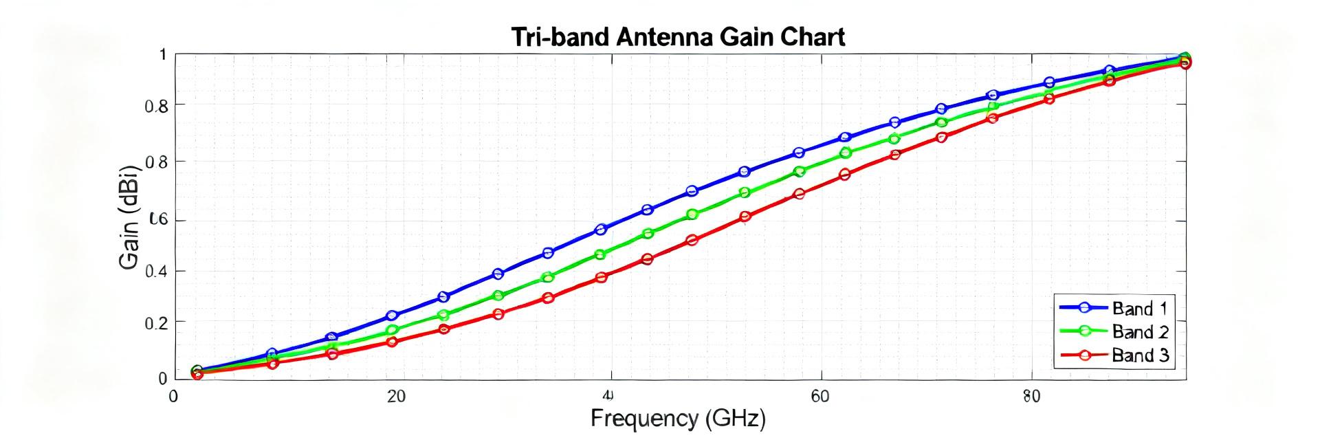
AANI-FB-0174-1 Datasheet: Measured Specs & Gain Charts
Data-driven hook: Measured lab validation of the AANI-FB-0174-1 shows a tri-band profile with peak on-band gains near 3.8 dBi (upper LTE band), efficiency typically 55–75% across the usable band, and …

AA428-210 AO2 Oxygen Sensor: Complete Specs & Data
The AA428-210 is a high-precision electrochemical oxygen sensor designed for industrial O2 monitoring and exhaust gas analysis. Engineered as a galvanic cell, it converts oxygen partial pressure into …
PTVS58VS1UR Datasheet Deep Dive: Key Specs & Ratings
2026-05-07 10:23:25
BCM5488RA7IPBG Datasheet Deep-Dive: Key Specs & Metrics
2026-05-01 10:13:18
PTVS5V0P1UP 600W TVS - Latest Lab Performance Brief
2026-04-26 10:17:16
PTVS5V0S1UR Technical Report: Specs & Performance Deep Dive
2026-04-14 10:17:24
PTVS5V0S1UR115 Datasheet: Complete Specs, Pinout & Ratings
2026-04-11 10:47:20
Read more